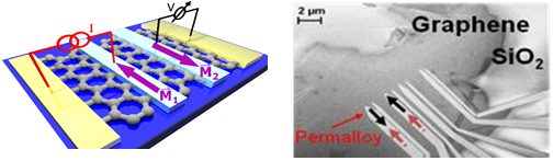
Charge and spin transport in graphene
Graphene is a monolayer of carbon atoms arranged into a two dimensional honeycomb lattice. Due to its exceptional band structure, charge carriers in graphene exhibit exciting physical properties which result in unconventional (magneto-)transport phenomena such as the room temperature quantum hall effect bagging the Nobel prize in 2010. Moreover, graphene is a promising material for spintronic applications [1] due to its high carrier mobility at room temperature and its long spin life time. We investigate the spin injection and the spin transport in graphene by using a nonlocal spin valve geometry [1, 2] with ferromagnetic electrodes as spin injector and detector. In addition to conventional sources for spin-polarized current such as ferromagnetic metals we also investigate ferromagnetic tunnel barriers which create two different barrier heights for spin-up and spin-down electrons [3].
References:
[1] W. Han et al., Nat. Nanotech. 9, 794 (2014).[2] D. Ilgaz et al., Phys. Rev. Lett. 105, 76601 (2010).
[3] J. S. Moodera et al., J. Phys.: Condens. Mat. 19, 165202 (2007).
Doped Graphene
In graphene which is doped by heteroatom substitution some of the carbon atoms are replaced by different atoms such as nitrogen or boron (as shown in Fig. 2). With Chemical Vapor Deposition (CVD) this can be achieved during the growth process and by changing the growth-parameters the level of doping can be varied. Doping leads to clear changes in the properties as for example an increase in charge carrier density and the possibility of opening a bandgap [1].

Figure 2: Schematic illustration of the lattice of doped graphene with the carbon atoms depicted as black nodes and the respective dopant in red, green or yellow.
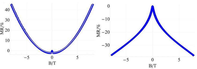
Furthermore, the change in resistance when applying a magnetic field – the magnetoresistance – changes its field-dependence and even the sign.
References:
[1] D. Wei et al., Nano Lett. 9, 1752 (2009).[2] M. Rein et al., ACS Nano 9, 1360 (2015).
Graphene Nanoribbons
Geometrically confining graphene into narrow ribbons (Graphene Nanoribbons - GNRs) will give rise to new phenomena unknown in extended graphene flakes and films. They occur because the edges in a system of finite size break translational invariance and thus, break also the equivalence of the two triangular Bravais lattices that build the hexagons. Hence, GNRs have been theoretically predicted to exhibit a band gap that can be tuned by tailoring their width and edge geometry (zigzag/armchair, Fig. 4) [1]. However, this tuning demands a well-controlled production process with plenty of opportunities for novel geometries. The most intuitive way to produce such GNRs is to simply slice Graphene or Carbon nanotubes (CNT) into GNRs by means of a top down fabrication method such as high resolution electron beam lithography [3] or unzipping of CNTs [4]. However, GNRs produced by top down approaches can hardly reach a width < 10 nm. In addition to that, the crucial edge structure cannot be controlled and is therefore likely a mixture between armchair and zigzag edges.
For precise edge structures and narrow widths (< 3 nm), a bottom up synthesis approach is needed. The pioneering approach of our collaborators from the Max Planck Institute for Polymer Research contains [5] cyclodehydrogenation and planarization of polyphenylene polymer precursors either in solution or on a metal substrates. These atomically perfect GNRs sparked intensive research on their fundamental properties as well as their potential for applications. The Kläui-lab as well as several groups at the MPIP are actively involved in fabrication, characterization and device production of a broad range of GNRs such as armchair GNRs with 5,7 and 9 atoms in the width direction.
These GNR allow combine matchless mobilities combined with the advantages of being a pure 2D material as well as a broad tunability and control of electronic and magnetic properties.
The investigation of the charge and spin transport in GNR will be carried out with chemically synthesized and atomically well-defined GNRs with a variety of lengths, widths and edge structures. These samples will be examined by optical measurements in close collaboration with the Group of Dr.Hai Wang and with low temperature transport measurements.
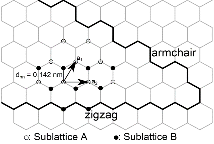
Figure 4: Armchair- and zigzag-edges in graphene. a1 and a2 denote the basic vectors of the triangular Bravais lattice. dnn = 0.142 nm is the lattice constant.
References:
[1] J. Cai et al., Nature (London) 466, 470 (2010).[2] O. Yazyev, Rep. Prog. Phys. 73, 056501 (2010).
[3] L. Tapasztó et al., Nat. Nanotechnol 3, 397 (2008).
[4] D. Kosynkin et al., Nature (London) 458, 872 (2009).
[5] A. Narita et.al, The Chemical Record, 15, 295 (2015).
Turbostratic Graphene
Besides single layer graphene, few- and multilayer systems exhibit also exciting properties. In turbostratic graphene stacks the layers are rotated with respect to each other leading to an electronic decoupling. It is thus a promising candidate to combine the electronic properties of single layer graphene with the robustness of graphitic microstructures. The common way to produce high quality turbostratic graphene is the epitaxial growth on the C-face of silicon carbide [1]. Alternatively, a plasma arc process yields discs comprised of 60 - 150 graphene layers. They typically exhibit large charge carrier mobilites of 105 cm2/Vs and show 2D transport features, such as weak localization [2], demonstrating the effective decoupling of adjacent graphene layers.
References:
[1] H. Hibino et al., J. Phys. D Appl. Phys. 45, 154008 (2012).[2] N. Richter, Y. R. Hernandez et al., arXiv:1301.6087 (2013).