In a wide variety of systems, the electrical resistance of a structure or thin film is dependent on the magnetic state, leading to a range of different effects which are classed as magnetoresistance (MR) [1]. Not only does the characterization of these effects provide very important information regarding the fundamental physical properties of a system, but they are vital experimental tools: for example the anisotropic magnetoresistance (AMR) effect can be employed to electrically detect the presence of magnetic domain walls in certain systems. Furthermore, MR is a vital technological component of a range of sensing technologies. Famous examples include the Nobel prize winning effect, giant magnetoresistance (GMR) and the tunneling magnetoresistance effect (TMR) employed in modern hard-disk drive read-heads, both of which occur in layered systems. For other applications such as multi-turn counting, we investigate novel domain wall based sensors relying on AMR, in collaboration with industry [2].
When spin - polarized currents interact with magnetic domain walls, different exciting effects occur: (i) the current manipulates the domain wall and can push it (spin transfer torque) or (ii) the domain wall can manipulate the spin-polarized current and for instance lead to scattering. The latter effect leads to the so called intrinsic domain wall magnetoresistance (DWMR) that stems from the scattering of the spin polarized conduction electrons by the non-collinear spin structure in a domain wall [1]. Theory predicts different sizes and signs of the resistance contribution of the domain wall, but generally it is predicted to scale with 1/d2 (d is the domain wall width) [1, 3-4], thus small systems with narrow domain walls are needed.
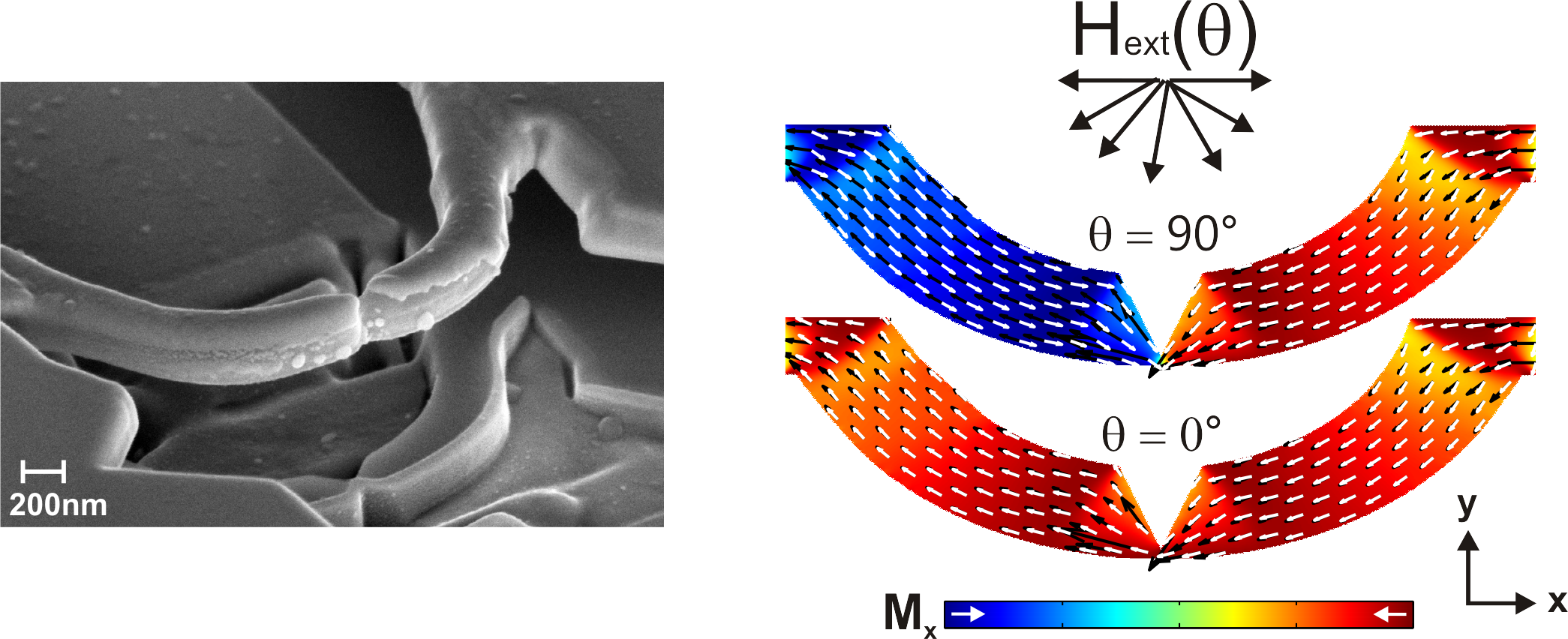
To this end, half-ring shaped magnetic nanocontacts, that contain a constriction notch, are investigated (see figure). Starting with a constriction of about 100 nm, the width can be continuously reduced via electromigration (EM) [5], with each EM step followed by magnetoresistance measurements. Our setup allows for in-situ growth and measurements in UHV-conditions to enable the study of intrinsic effects without the influence of contaminants. In the low-resistance regime up to 1 kOhm the anisotropic MR is the leading contribution [6], with intrinsic DWMR emerging only for very narrow domain walls. At higher resistance values in the ballistic and tunneling regime large MR effects ( >50% ) are observed, that can be attributed to the presence of a domain wall in the nanocontact [7]. Our results can be reproduced by recent atomistic calculations for different atomic configurations of the nanocontact, highlighting the importance of the detailed atomic arrangement for the MR effect [8]. In addition to DWMR, these magnetic nanocontacts offer a unique way to investigate a variety of other magnetic effects in confined geometries such as the interplay between transport and spin structure. Furthermore we are able to characterize the energetic landscape of the strong domain wall pinning potentials due to notches including their angular dependence and symmetry for this constriction size regime, which is not easily accessible using conventional lithographic approaches [9]. Finally the nanocontacts can also be opened to form nano-gaps that can then be filled with molecules or graphene nanoribbons to measure the transport across a single molecular entity.
References:
- H. Marrows, Advances in Physics 54, 585 (2005).
- Borie et al, Phy. Rev. Applied 8, 024017 (2017).
- Viret et al., Phys. Rev. B 53, 8464 (1996).
- M. Levy and S. Zhang, Phys. Rev. Lett. 79, 5110 (1997).
- Hoffmann et al., Appl. Phys. Lett. 93, 043118 (2008).
- Patra et al., Phys. Rev. B 82, 134447 (2010).
- von Bieren et al., Phys. Rev. Lett. 110, 067203 (2013).
- Achilles et al., Phys. Rev. B 84, 054418 (2011).
- Reeve et al., J. Phys.: Cond. Mat. 26, 474207 (2014).